

8. Subwavelength control of light in semiconductor nanowires.
Contact person:
Francesco Rossella
Stefano Roddaro
The manipulation of light below the diffraction limit attracts much attention owing to its potential impact on sensing, microscopy, and computation and communication technologies. Nanowire-based hybrid
electronic/plasmonic systems are possible building-blocks for novel nano-optoelectronic chips
embedding multiple functionalities. Individual semiconductor nanowire devices have been engineered,
and have allowed us to demonstrate a novel technique for the realization of subwavelength light
sources operating at 1 GHz.
|
|
|
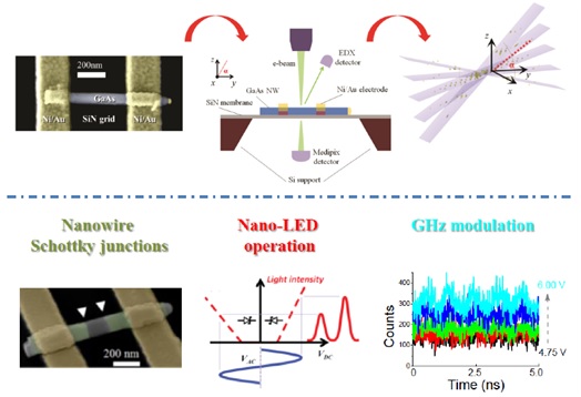
Top panel: Electron diffraction
tomography in a single nanowire-based device. N-doped GaAs NWs were deposited onto a SiN
membrane and contacted by two Ni/Au electrodes. The SiN membrane, transparent to electrons, is
supported by a thicker silica membrane with a central hole allowing the electrons to pass through the sample, which can be tilted by an angle α around the x-axis. Diffraction patterns were measured at different angles, and merged via dedicated software to obtain a 3D reconstruction of the reciprocal lattice. Bottom panel: Fast light emission in nanoscale point sources. In devices with two Schottky junctions, upon large bias excitation at frequency that alternatively drives both the Schottky barriers in the reverse breakdown regime.
F. Rossella, V. Piazza, M. Rocci, D. Ercolani, L. Sorba, F. Beltram, and S. Roddaro, GHz Electroluminescence Modulation in Nanoscale Subwave length Emitters, NanoLett., 16, 5521-5527
(2016)
J. David, F. Rossella, M. Rocci, D. Ercolani, L. Sorba, F. Beltram, M. Gemmi, and S.
Roddaro Crystal Phases in Hybrid Metal–
Semiconductor Nanowire Devices, NanoLett., 6, 2336–2341 (2017)
|
|
|
|
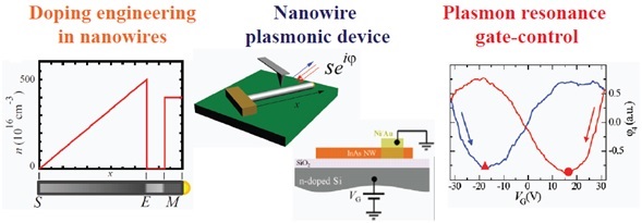
Linear modulation of the carrier density profile as a
function of the axial position along an InAs nanowire. An intermediate-doping segment was introduced
in the growth sequence and used as marker for the s-SNOM maps. The resulting graded-doping NW is
sketched at the bottom of the diagram. NWs were deposited on a SiO2/Si substrate and contacted by
a Ni/Au electrode. The bulk silicon was degenerately n-doped and thus can act as a back-gate upon
application of a bias voltage. The laser impinging on the tip was vertically polarized with the wave
vector forming an angle of 30° with the surface of the NW. The amplitude and phase of the reflected
beam are detected using an interferometricpseudoheterodyne technique, demodulated at the fourth
harmonic of the tip tapping frequency and used to reveal the local dielectric response of the NW.
Phase modulation was achieved as a function of the gate voltage. A strong hysteresis was observed by
sweeping the gate voltage from low to high values and back.
A. Arcangeli, F. Rossella, A.
Tomadin, J. Xu, D. Ercolani, L. Sorba, F. Beltram, A. Tredicucci, M. Polini, and S. Roddaro Gate-Tunable Spatial Modulation of Localized
Plasmon Resonances, NanoLett., 16, 5688–5693 (2016)
|
|