Nanofabrication by focused ion and electron beams
People
Gian Carlo Gazzadi
Stefano Frabboni
Nanofabrication by focused ion and electron beams is performed with a dual beam workstation, combining a field-emission SEM and a Ga-ion FIB, and equipped with gas injection systems.
Two main approaches are followed:
- one is the nanomachining and nanopatterning by ion milling or bylow-dose ion irradiation, and
- the other is the beam-induced deposition of gas precursors, using either electrons or ions.
These nanofabrication techniques are extremely versatile since they are performed directly on the sample without multiple processing steps (as in standard lithography), and can be applied to any solid material.
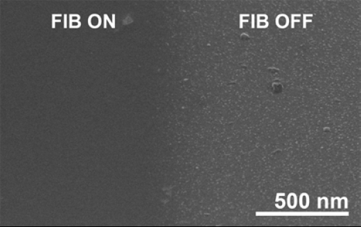
In fig.1, an example of FIB nanopatterning is shown. A Si surface, functionalized for the grafting of magnetic nanoparticles, is patterned by low-dose FIB irradiation. The functionalization layer is removed in the FIB-patterned areas preventing the grafting of the nanoparticles.
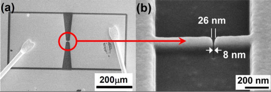
In fig. 2, the fabrication of nanogap Au electrodes demonstrates the high resolution capability of FIB lithography. Electrodes are patterned on an Au film by FIB milling, starting from the big contact pads (fig. 2a) down to the nanogap tips (fig. 2b). Decreasing FIB currents are used for each step, corresponding to increasing beam resolution. A final gap of 8 nm is obtained, a result achievable only by the most advanced e-beam lithographies.
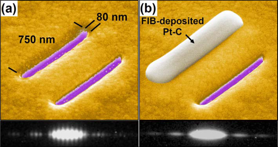
In fig. 3, the combination of FIB milling and deposition is employed for the realization of the double slit Feynman experiment at the nanoscale. Two nanoslits are opened on an Au-coated silicon nitride membrane, and the corresponding electron diffraction pattern is measured with a TEM (fig. 3a). The further step is to cover one of the slits with a FIB-deposited Pt-C nanostrip, and measure the single slit interference pattern (fig. 3b).
Our group is strongly involved in the study of focused electron beam-induced deposition (FEBID). This additive nanolithography produces nanostructures that can be employed in functional nanodevices or in the study of fundamental properties at the nanoscale.
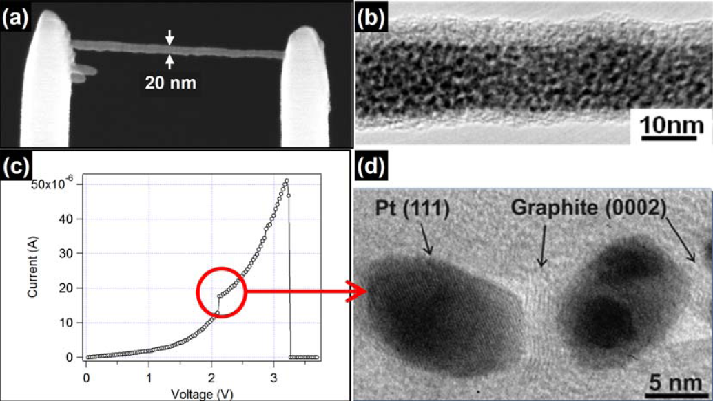
In fig. 4, the growth of suspended nanowires from Pt-metallorganic precursor and the study of their structural and electrical properties are presented. The nanowires are deposited across two pillar-electrodes (fig. 4a) and consist of small Pt nanograins (2-3 nm) homogeneously distributed inside a carbonaceous matrix (fig. 4b). They are highly resistive and under an increasing electrical current (fig. 4c), Pt aggregation into larger grains (10-15 nm) and carbon matrix graphitization are observed (fig. 4d). Recently we have started the characterization of a new cobalt precursor for the growth of magnetic nanostructures. First results show that the as-deposited wires are non-magnetic and undergoferromagnetic transition after 400 °C thermal annealing.
 |
|
Fig. 1. FIB Nanopatterning by low-dose ion irradiation. FIB irradiation, on the left, removes the functionalization layer and magnetic nanoparticles attach only on the right side.
|
 |
|
Fig. 2. Fabrication of Au nanogap electrodes by full-FIB lithography process. (a) The contact pads are patterned first, with high current beam. (b) The nanogap electrodes are patterned in the final step with the smallest beam current.
|
 |
|
Fig. 3. Double-slit Feynman experiment at the nanoscale. (a) Two nanoslits are opened by FIB milling on a thin membrane. (b) One of the slits is covered by Pt-C FIB deposition. The corresponding interference patterns (bottom) are measured with a TEM.
|
 |
|
Fig. 4. (a) Suspended Pt-C nanowire grown by FEBID. (b) Nanowire structure analyzed by TEM: Pt nanograins (dark) are embedded in a carbonaceous matrix (bright). (c) I-V characteristic of the nanowire: as the current increases, Pt aggregation and matrix graphitization are observed (d).
|