SPINTRONICS AND NANO-DEVICES
People
Alberto Ghirri
Marco Affronte @ Modena
Spintronic devices interconvert spin to charge information and nanostructured carbon systems turn out to be a unique platform to build hybrid devices at the molecular scale. We aim at realizing novel spintronic nano-architectures where the electrical current is controlled by the properties of active monolayers, molecules or nanoparticles in proximity with the graphene layer.
Hybrid Graphene – nano Magnet Devices for Spintronics
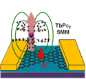
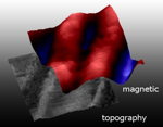
We explored different strategies to graft molecular nanomagnets on carbon surfaces (see MAGNETIC MOLECULES & NANOPARTICLES AT SURFACES). Here, we employed TbPc2 molecules appositely functionalized with pyrene groups that selectively graft to graphene, studying the π-orbital mediated interaction by means of micro-Raman spectroscopy and Atomic Force Microscopy (see Fig. 1). We have designed and realized a hybrid device by decorating a graphene nanoconstriction (behaving as a quantum dot) with TbPc2 magnetic molecules. The anisotropic magnetization reversal of the molecules in proximity with graphene is detected by the magnetoconductivity. This prototype depicts the behavior of novel class of molecular spin valve with sensitivity at the single-molecule level (see Fig. 2).
  |
|
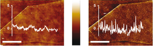
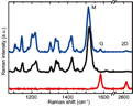
Fig 1. Atomic Force Microscopy topography image and height profile of a graphene flake before (a) and after (b) deposition of TbPc2 magnetic molecules. (Scale bars = 3 μm). (c): Raman spectra of the pristine graphene flake (red), powder of TbPc2 molecules and hybrid system graphene+TbPc2 (blue).
|
   |
|
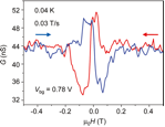
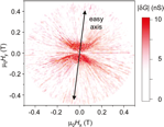
Fig 2. (Left) Pictorial view of the device. The graphene nanocostriction is coupled to the magnetic moment of the TbPc2 magnetic molecules deposited on its surface. (Center) Magnetoconductivity of graphene + TbPc2 obtained at a fixed backgate voltage. The blue curve is the magnetoconductivity under increasing field (trace), while for the red curve the field is decreasing (retrace). The observed hysteresis is given by the magnetization reversal of the TbPc2 molecules in proximity with graphene. (Right) Color plot of the difference between trace and retrace) for all directions of the magnetic field in the plane of graphene. The border between the red regions and the noncolored ones represents the fields at which the hysteresis loop is closing. The behavior is typical for magnetic systems with uniaxial anisotropy and the easy axis is indicated. Along the hard direction (perpendicular to the easy axis) no hysteresis is observed as the magnetic field is not high enough to reverse the magnetization of the system.
|
HALL PROBE MAGNETOMETRY.
1. Hall magnetometry with QD PPMS.
We have implemented the Hall micro-probe magnetometry technique in the Quantum Design Physical Properties Measurements System (PPMS). This technique allows us to detect signals from very tiny crystals of magnetic materials, typically 10 – 100μm in size. Since Hall devices can be used with the standard Resistivity puck, with the Horizontal Rotator and with the Helium-3 insert, various kinds of magnetization measurements can be performed down to 0.3~K and below. In the technical report QD 1084-701 we briefly report on the experimental set-up will as well as selected results to illustrate its capabilities.
Reference: 1084-701 technical support
2. Fabrication of Hall nano-probes.
We fabricated Hall magnetometers by patterning Gold and Si-doped GaAs films down to 100x100nm² active area by Focused Ion Beam. Electrical characterization shows that the magnetic flux sensitivity of GaAs probes is better than 10-2 φ0 at room temperature while Hall nano probes made of gold can work down to liquid helium with magnetic flux sensitivity 10-1 φ0.
3. Hall probe microscopy
We use Scanning Hall-probe microscope (SHPM) by Nanomagnetics Inc inserted in Quantum Design PPMS cryo-magnetic setup. In scanning Hall-probe microscopy (SHPM), highly sensitive Hall probes detect the intensity of the stray magnetic fields and can be used to scan the surface of the sample. The approach of the probe to the surface is realized by means of a conventional electron tunneling feedback. The tip is a gold pad, which is placed near the Hall cross (at a distance of 13μm). STM images can thus be acquired simultaneously with SHPM. The sample must be tilted by small angle (1°) in order to prevent the other parts of the sensor to crash on the surface. Therefore, the minimum distance between the Hall probe and the surface is typically 250nm. The tunnelling feedback is not longer necessary upon, and the controller allows scanning also at other user-defined distances from the surface. The scan area is 56x56μm² at room temperature and it shrinks down to 4.5x4.5μm² at T=2K, due to the temperature dependence of the piezotube motions.
 |
|
Magnetic imaging of prussian blue nanoparticles grafted on FIB-patterned substrates. A. Ghirri, A. Candini, M. Evangelisti, G. C. Gazzadi, M. Affronte, F. Volatron, D. Brinzei, B. Fleury, L. Catala, C. David, and T. Mallah. SMALL 4, 2240–2246 (2008).
|
Publications
Deposition of Functionalised Cr7Ni Rings on Graphite from Liquid Phase.
A. Ghirri, V. Corradini, C. Cervetti, A. Candini, U. del Pennino, G. A. Timco, R. G. Pritchard, C. A. Muryn, R. E. P. Winpenny, and M. Affronte
Adv. Funct. Mat. 20, 1552-1560 (2010).
Surface-Enhanced Raman Signal for Terbium Single-Molecule Magnets Grafted on Graphene.
M. Lopes, A. Candini, M. Urdampilleta, A. Reserbat-Plantey, V. Bellini, S. Klyatskaya, L. Marty, M. Ruben, M. Affronte, W. Wernsdorfer, and N. Bendiab
ACS Nano 4, 7531-7537 (2010).
Graphene Spintronic Devices with Molecular Nanomagnets.
A. Candini, S. Klyatskaya, M. Ruben, W. Wernsdorfer, and M. Affronte
Nano Lett 11, 2634-2639 (2011).